Static Timing Analysis (STA) is a method used to evaluate the timing in a design. For FPGA designs, it is used by the place and route tools to locate the components, and to ensure that the timing has been met. STA is based upon synchronous design techniques, i.e. designs that have a clock. Believe it or not, there were asynchronous computers many years ago, and this technique wouldn't be useful for them.
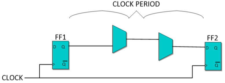
Static timing analyzers check the timing from register outputs or device inputs, through any combinatorial logic, and into the next register input or a device output. Consider the following path:

In this path, the data flows from the output of FF1 with the clock to Q output delay, through two combinatorial elements, and then must be set up to FF2. The frequency that this circuit would achieve is based upon these times. If the clock to Q were 2 nsecs, each of the logic elements were 3 nsecs, and the setup time were 2 nsecs, we would have a total delay of 10 nsecs, so the maximum frequency would be 1/10 nsecs = 100 MHz.
If the design were actually run at 80 MHz, or a period of 12.5 nsecs, then the excess amount, 12.5 nsecs - 10 nsecs = 2.5 nsecs, is referred to as the "slack".
The static timing analyzer performs this analysis through the entire design to determine the maximum frequency for the design, and to flag any errors, or "negative slack" that occurs and to report those paths.
It's important to understand that a static timing analyzer does not examine the logic in a design - the analysis is performed without any simulation of the design. For example, if in the circuit above clock enables were used to divide the clock rate in half, the static timing analyzer wouldn't know about this unless you informed it via a constraint. This is referred to as a "multicycle path" and is a valid method of meeting timing for large combinational blocks, for example arithmetic operations.
Modern static timing analyzers are quite sophisticated, and actually examine the delay through clock buffers and to each individual flip flops in a design, take into account clock jitter, routing, fanout, and other artifacts of the FPGA. With static timing analysis as the standard approach, it generally is no longer necessary to perform a back annotated (timing) simulation as long as the constraints are properly constructed and the STA output is examined thoroughly.
© Copyright 2018 Verien Design Group, LLC Concord, MA All Rights Reserved