3D Metal Printing System
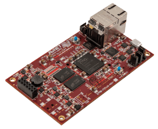
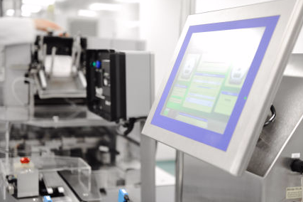
Verien led a team of four in the design of a 3D metal printing system which consisted of two FPGA designs, three board designs, and mechanical enclosures. The main FPGA is a Zynq Ultrascale+ MPSoC with six ARM cores running the application, with communications over Gigabit Ethernet and two Powerlink nodes allowing for real time synchronization and system expansion. This FPGA communicated to the second board with three Artix-7 FPGAs which implemented the laser interfaces.
The main FPGA interfaces to encoders for position information and receives packets of laser descriptors which specify firing the lasers using PWM with 10 nsecs of accuracy. All of this may be replicated and operated in synchronization allowing for modularization that controls an array of over 150 high powered lasers.
The system contains many essential interfaces: status and control of multiple 10KW power supplies to power the lasers, laser status and power monitoring, laser safety interlock, laser current control, the cooling subsystem, SATA (eMMC) drive, and others.
Zynq-Based Pulse Acquisition and Processing
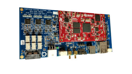
This Zynq XC7Z020 SOC based system is used for nanoparticle acquisition and analysis. It acquires raw pulse data from six sensors simultaneously, conditions the differential analog signals, and acquires the data into DDR memory at 80 Msamples/sec using three AD9269 dual ADCs. The FPGA then performs real-time extraction of the pulse characteristics - real time measurements of the acquired pulses. These measurements are packetized and DMA transferred to ping pong buffers in the DDR memory of the ARM processors. The pulse data can be programmably filtered or decimated prior to acquisition. An adaptive filtering scheme, based on IIR and moving average filters, was designed using Matlab / Simulink for determining the baseline of the signal prior to acquisition. The board design contains the six high-speed ADCs fed by a differential analog front end, a DAC used to generate pulses programmatically for testing purposes, and Ethernet connectivity to the host. The FPGA design makes heavy use of the internal AXI busses between the FPGA fabric and the processing subsystem for acquisition and processing.
True Random Number Generator
This system was based on the Zynq SOC and implemented a random number generator using a carrier card provided by the client. The carrier card had multiple entropy sources, reverse bias diode noise generators and geiger counters with radiation sources, which were acquired from by the FPGA and AD7885 ADCs, and this entropy was used to seed the random number generation. Random number generation was implemented in the FPGA fabric with data delivered to the ARM processing subsystem for later transfer to the host.
Zynq Based Magnetometers
This client develops ultraprecision magnetometers for government and industry. Two products were designed based on the Xilinx Zynq SOC. The Zynq contains dual ARM-9 processors, Gigabit Ethernet, USB, and a host of other features along with a generous helping of programmable logic. These designs were based on custom carrier cards for the MicroZED (pictured) running Linux and communicating to the host using Ethernet and USB. The FPGA functions include: modulation of the sensor via Direct Digital Synthesis (DDS), acquisition, IIR filtering, and demodulation using lock-in amplifiers, and control of multiple precision sensor heaters and other custom interfaces. Interfaces include the AD7176 ADC, AD7193 ADC, LTC2378 ADC, and AD5541A DAC. A specialized communications scheme was developed to allow synchronization and host access in a multi-board system.