website creation software


Image Processing and Camera Designs

This is a sample of some of our image processing and camera designs.  Besides the examples below, Verien has designed CCD, CMOS, and infrared cameras, as well as several frame grabbers.

Embedded Binocular Vision System

Embedded Binocular Vision System 
Based upon a TI DSP, this low cost embedded system provides image acquisition and processing from two CMOS sensors, video display, FLASH, SDRAM, I2C, real time clock, and Ethernet. The programmable logic provides most of the glue for the system: sync generation, an optical encoder interface, a PWM heater controller, and other necessary functions.  The application was a security camera for revolving doors.
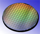
Image Processing System for Wafer Repair 
This system is used for the inspection of wafers during plasma etch and essentially uses each pixel of a CCD as an interferometer. The client needed to have a camera with thermally controlled CCD array in a very small package, and desired to connect up to four of these cameras to a single frame grabber with image processing performed on the live data. The result was the development of an actively cooled camera (using Peltier coolers) approximately 1" x 2" x 3" in size and which contained the A/D and several DACs, all CCD timing generation and control, as well as a differential interface back to the frame grabber. The frame grabber captures four live video streams, performs image processing on the streams, and then transfers the data to host memory. 

Wafer Repair Image Processing System
FPGA Ultrasound Processing

Cardiac Ultrasound Image Processor 
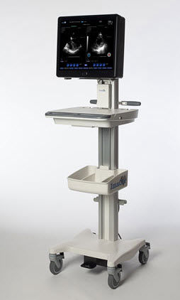
This FPGA performs the real-time digital signal processing of cardiac ultrasound images. Implemented in a low-cost Xilinx device, it provides 17 stages of 1D and 2D processing at 160 MHz (40 MHz sample rate), a scatter/gather DMA controller, and PCI bursting target and initiator interfaces. The client came to Verien with the DSP algorithms implemented in C; Verien redesigned these in VHDL and regression tested the output data from the C version against the FPGA simulation. The processing pipeline includes symmetric FIR filters with decimation, gain correction, display brightness compensation,  and programmable region of interest.  Xilinx PBlocks were used to achieve the 160 MHz rate in a slowest speed grade device.

CT Scanner Products 
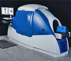
These FPGAs provide many of the processing stages for CT scanner used for baggage inspection. The design was mixed VHDL and with MatlabTM / Simulink blocks integrated through Xilinx System Generator for DSP tool. The processing pipeline runs at a data rate of 133 MHz and provides in excess of 1.5 GBytes/sec of DDR2 bandwidth. Development in Matlab / Simulink provided for a rich DSP environment. Simulink blocks from the Xilinx blockset were integrated into a top-level VHDL, and then the Simulink and VHDL simulation data was regression tested.

Verien has designed three other products for this companies CT product line, all implemented in low-cost Spartan-6. These cards plus FPGAs all provide a remote I/O capability, interfacing various I/O interfaces to the host via proprietary optical links. Many of these slower I/O interfaces use MODBUS with MODBUS implemented directly in the fabric. Two of the interfaces perform closed loop motor control in the FPGA hardware.

FPGA CAT Scanner Processing

© Copyright 2018 Verien Design Group, LLC  Concord, MA All Rights Reserved