bootstrap responsive templates


Unit Cost vs. Development Cost in FPGA Projects

Years ago, when ASICs and gate arrays were the medium for custom ICs, one had to develop the chip and the full product all at once, and get it right the first time. Now with FPGAs, there are more options, and these options can affect your development cycle which determines your development and unit costs. With FPGA-based projects, there is a relationship between the unit cost and development cost that must be considered up front and take into account several factors:
  1. Size of the project 
  2. Software design complexity 
  3. Software design complexity 
  4. Mechanical design complexity
  5. Availability of funds


Size of the Project

For small and medium projects without much software and mechanical design complexity, it is still may be best to skip the prototype stage and go right for the production units. There remains, however, a tradeoff between unit and development costs; if the product is intended to be very high volume, then it makes economic sense to spend the time reducing the required components and component costs as much as possible. This increases development costs slightly, but for high volume products, the payback for this can be in the first year or two. Consider a product that ships 5,000 units per year. If one could shave $5 off of the bill of materials cost, it would cover $25,000 in development costs!


Software Design Complexity

If the product requires a significant software development effort, and this could either be host level software or embedded software running on an SOC like the Zynq, then this can have an impact on the unit / development cost tradeoff. Reflecting back on the days of ASICs again, for ASIC-based products, while the software developers were free to write the necessary code for a new product from the project start, they generally couldn’t test a line of code until the product was complete, and this can have a significant impact on total development time. 

For FPGA-based products, there is another path – the development of a Proof Of Concept (POC) system using an off-the-shelf evaluation card. This can provide a platform for software development prior to the actual hardware being completed.


Use of Evaluation Cards

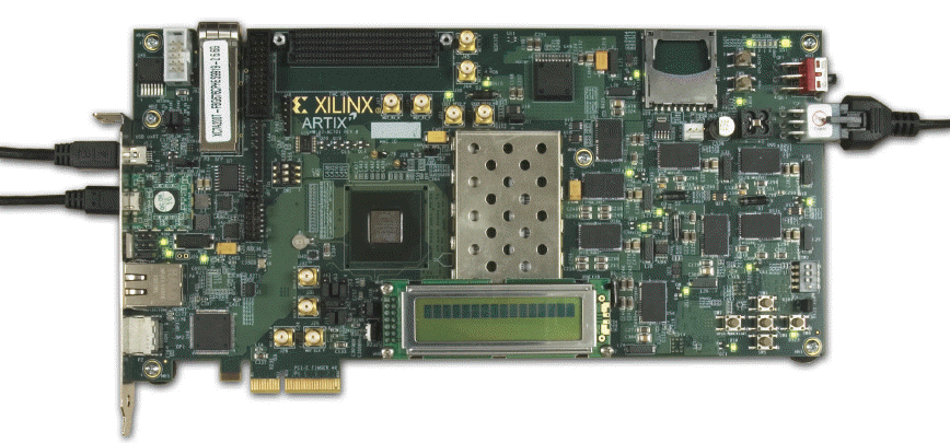
The FPGA evaluation cards available today come in many sizes and loaded with bells and whistles. There are the straight-up FPGA cards like the Xilinx AC-701:
AC-701 Evaluation Card
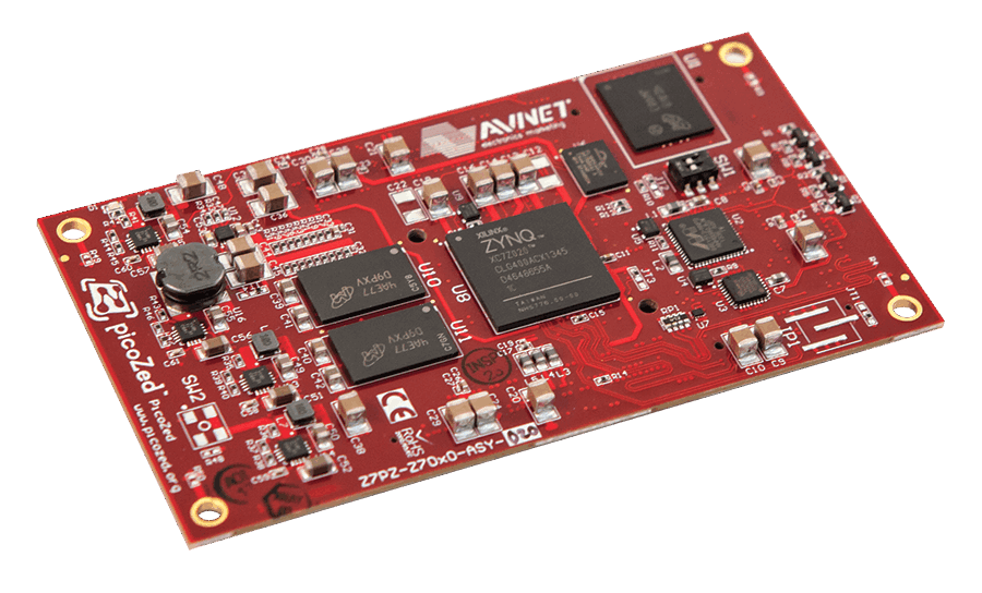
and embedded FPGA cards like the Avnet PicoZED, containing a Zynq FPGA with dual ARM processors, a plethora of I/O, and on-board flash and DDR memory:
PicoZED Evaluation Card

These SOC cards generally contain a high-density connector which provides the connections to the FPGA fabric and the I/O (Gigabit Ethernet, USB, serial I/O, PWM, SPI, etc). Cards like the PicoZED are referred to as System On Modules (SOMs) which require a carrier card for power and the I/O connectors. The vendors provide generic carrier cards which can be used to create a development platform.

One of the challenges when developing a POC system is when the final product is a data acquisition system, that is, it contains ADCs which won't be available in an off-the-shelf evaluation card. In this case, it may be possible algorithmically generate the ADC data in the FPGA, or to download the data to the card prior to running the application.

By using an evaluation card as a POC system, generally some portion of the FPGA design needs to be completed, but while the actual hardware (PCB design) may be months from completion, the debug of the software can get started months early using the POC system. The POC system will be software compatible with the final hardware since it’s basically the same FPGA design – a huge advantage.

Mechanical Design Complexity

For high-volume development which is space constrained and/or includes the development of an enclosure, it generally makes sense to develop the hardware in two passes. The first pass is completely custom much like the final design, but without constraining the design for size and without the enclosures, which probably won’t be ready at this time anyway.  Generally, cost optimization is relaxed for this first pass, as well, since the goal is to get something quickly for software development. The system is then redesigned to fit into the final enclosure design and with the costs shaken out.


Overall Design Complexity

For highly complex designs, and in particular, mixed signal data acquisition systems with high precision requirements, it is often necessary to perform multiple passes to achieve the noise goals for the final product.  When attempting to read microvolt levels with millivolts of radiated or conducted noise, determining the sources of the noise into the analog front end can be impossible using simulation techniques - one just needs to build it.  Unfortunately, in order to gauge the level of noise in the system, one needs to build the real thing - or as close to the real thing as possible.  Depending upon the nature of the product, it still might make sense to use an evaluation platform, to get the software development started.


Funding Driven

When designing the first product for a startup, it is often necessary to design it in two passes based upon available funding. In this case, the POC system is really being designed to prove the system to investors in order to obtain the necessary funding for the final, high-volume system. Generally, the POC system is not space and unit cost constrained, but is development cost constrained. As such, cost and space minimization aren’t taken into account for the first pass. Note that the total development time may be a longer since it requires two passes, but is necessary to reach the end goal.
Resources

Tech Notes
IP Cores

Contact

Email: info@verien.com 
Phone: 978-405-3102 

© Copyright 2018 Verien Design Group, LLC  Concord, MA All Rights Reserved