Mobirise


Communications Designs

This is a sample of some of our communications designs.

4 lane, Gen2 PCI Express Card Design

4-Lane Gen2 PCI Express Card 
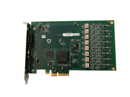
This client needed a four lane, Gen2 PCI Express card for a security application. Designed for a Xilinx 7-Series device, a cost effective Artix-7, it achieved a measured 1.25 GBytes/sec of bandwidth using a custom chain linked list DMA engine. The board FPGA interfaced to 8 ADCs, an LTM9008, via LVDS interfaces.  

The Real Time Data Interface 
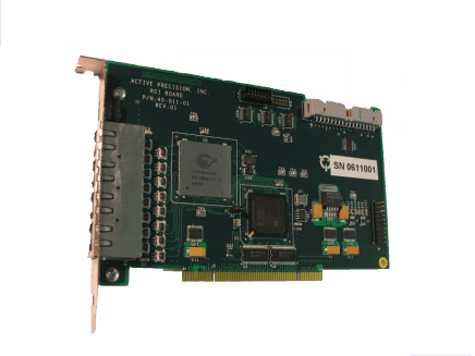
The RDI is a custom PCI card used for real time distributed motion control systems. This PCI card provides four 500 Mbit/sec links over CAT cable for reliable packet communications, eight linked-list DMA engines which allow real-time scheduled transfers, and nanosecond-class box-to-box synchronization for distributed real-time control operations. This custom packet protocol, architected by Verien, breaks transfers into small packets to have a deterministic real-time latency, and uses cut-through for higher priority transfers. Transfers can be either reliable (acknowledged and retried in hardware) or UDP-style with a sequence number provided at the destination.  A pool of DMA engines is used to transfer between host memory and resources on any box in the system with a known latency.

Real Time Motion Control FPGA and Card Design
Remote I/O FPGA and Card Design

Remote I/O Cards 
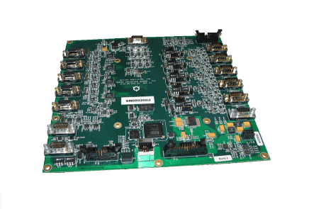
Verien has designed a number of remote I/O cards for different clients and applications.  These cards take in slower I/O, encapsulate the I/O into packet data, and send it across an optical link at gigabit speed to the second card where the I/O is replicated.  These are generally designed with a custom link protocol as it is minimizes development costs over the use of a standardized interface.  The high-speed transceivers in the Xilinx Artix-7 or Altera (Intel) Cyclone V families provide a cost effective solution.  The slower I/O can include a number of different types of sources and destinations: UART serial I/O, A/D, D/A, SPI, general purpose I/O, relay I/O, and others.
Dual Gigabit Communications Link
This client needed a large packet data mover for an industrial imaging application. The result is a dual 1.3 Gb/sec optical card that achieves a measured 220 Mbytes/sec over 64-bit, 66 MHz PCI. The FPGA provided all header encapsulation and packet processing. Out of band mailbox transfers are provided as a means of communication between the boxes.

Reliable Communications Link IP Core

This client needed a reliable communications link over differential pair for box to box communications.  Verien designed an IP core with a frame-based protocol over a single RS-485 differential pair.  All communications is error checked and acknowledged, and with automatic retries performed by either the master or the slave.  All errors are treated as soft, recoverable errors until an error limit is reached, as determined by an error counting algorithm.

CT Scanner Rotor / Stator Comm Link

This card was a part of a CT scanner and communicated  from the stator assembly to the rotor assembly over a proprietary optical link.  The CT data was sent from the rotor to the stator with all packet formatting and processing performed in the FPGAs.  Additional FPGA control included: closed loop motor control over MODBUS (with MODBUS protocol and motor control performed in the FPGA), ADC interfaces, power monitoring, PWM temperature sensors, numerous serial ports, and other remote I/O capability.  Verien designed three cards and FPGAs very similar to this one for this long-term client.

© Copyright 2018 Verien Design Group, LLC  Concord, MA All Rights Reserved